General Description
This device contains two independent negative-edge-triggered J-K flip-flops with complementary outputs. The J and
K data is processed by the flip-flop on the falling edge of
the clock pulse. The clock triggering occurs at a voltage
level and is not directly related to the transition time of the
falling edge of the clock pulse. Data on the J and K inputs
may be changed while the clock is HIGH or LOW without
affecting the outputs as long as the setup and hold times
are not violated. A low logic level on the preset or clear
inputs will set or reset the outputs regardless of the logic
levels of the other inputs.
-26%

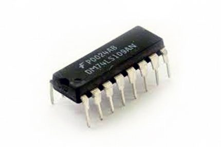
74LS109 Dual J-K Positive-edge-triggered Flip-Flop IC
Original price was: ₨ 145.₨ 120Current price is: ₨ 120.
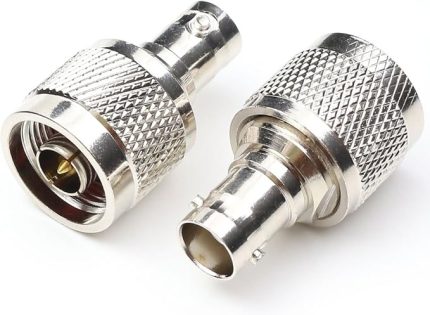
N Male Connector to BNC Female connector
Original price was: ₨ 1250.₨ 850Current price is: ₨ 850.
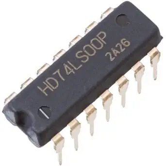
74ls112 ic
Original price was: ₨ 135.₨ 100Current price is: ₨ 100.
Description
Reviews (0)
Shipping & Delivery


Related products

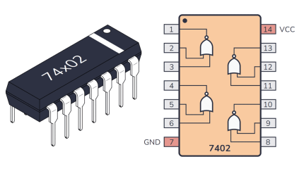
NOR Gate IC 74LS02 Quad 2-input
Operating voltage range: +4.75 to +5.25V
Maximum supply voltage: 7V
Maximum current allowed to draw through each gate output: 8mA
TTL outputs
Low power consumption
Maximum ESD: 3.5KV
Typical Rise Time: 15ns
Typical Fall Time: 15ns
Operating temperature :0°C to 70°C
Storage Temperature: -65°C to 150°C
Operating temperature: 0°C to 75°C
Pin Number Description
NORGATE 1
2 1A-INPUT1 of GATE 1
3 1B-INPUT2 of GATE 1
1 1Y-OUTPUT of GATE1
NORGATE 2
5 2A-INPUT1 of GATE 2
6 2B-INPUT2 of GATE 2
4 2Y-OUTPUT of GATE2
NORGATE 3
8 3A-INPUT1 of GATE 3
9 3B-INPUT2 of GATE 3
10 3Y-OUTPUT of GATE3
NORGATE 4
11 4A-INPUT1 of GATE 4
12 4B-INPUT2 of GATE 4
13 4Y-OUTPUT of GATE4
SHARED TERMINALS
7 GND- Connected to ground
14 VCC-Connected to positive voltage to provide power to all four gates
SKU: 0401 Categories: Discrete Electronic Components, ICs, Logic Gates Tags: 2input, 74LS02, Gate, IC, NOR, quad
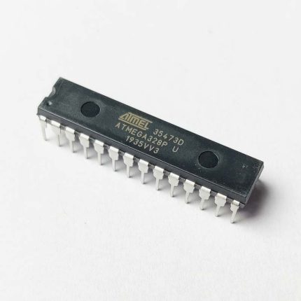
Original Atmega328 28 Pin Atmega328p-pu Microcontroller
Specifications of Atmel 8 Bit 28 Pins Microcontroller ATMEGA328P Microchip:
4.5V-5.5V operating range
Up to 20MHz
Part: ATMEGA328P-AU
32kB Flash program memory
1kB EEPROM
2kB Internal SRAM
Two8-bit Timer/Counters
One16-bit Timer/Counter
RTC with separate oscillator
6 PWM Channels
8 Channel 10-bit ADC
Serial USART
Master/Slave SPI interface
2-wire (I2C) interface
Watchdog timer
Analog comparator
23 IO lines
Data retention: 20 years at 85oC/ 100 years at 25oC
Reviews
There are no reviews yet.