General Description
This device contains two independent negative-edge-triggered J-K flip-flops with complementary outputs. The J and
K data is processed by the flip-flop on the falling edge of
the clock pulse. The clock triggering occurs at a voltage
level and is not directly related to the transition time of the
falling edge of the clock pulse. Data on the J and K inputs
may be changed while the clock is HIGH or LOW without
affecting the outputs as long as the setup and hold times
are not violated. A low logic level on the preset or clear
inputs will set or reset the outputs regardless of the logic
levels of the other inputs.
-26%

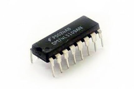
74LS109 Dual J-K Positive-edge-triggered Flip-Flop IC
Original price was: ₨ 145.₨ 120Current price is: ₨ 120.

N Male Connector to BNC Female connector
Original price was: ₨ 1250.₨ 850Current price is: ₨ 850.
74ls112 ic
Original price was: ₨ 135.₨ 100Current price is: ₨ 100.
Description
Reviews (0)
Shipping & Delivery


Related products
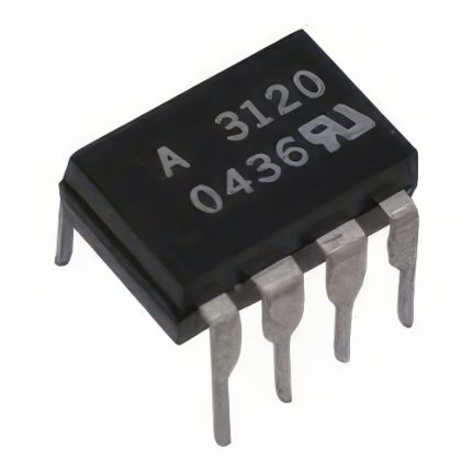
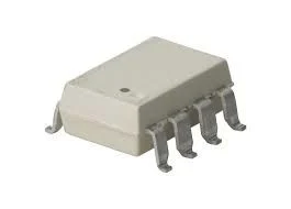
A3120 IC HCPL3120 DIP
2.0 A Minimum Peak Output Current
15 kV/µs Minimum Common Mode Rejection (CMR) at VCM = 1500 V
0.5 V Maximum Low-Level Output Voltage (VOL) Eliminates the Need for a Negative Gate Drive
ICC = 5 mA Maximum Supply Current
Under Voltage Lock-Out Protection (UVLO) with Hysteresis
Wide Operating VCC Range: 15 to 30 Volts
500 ns Maximum Switching Speeds
Industrial Temperature Range : -40°C to 100°C
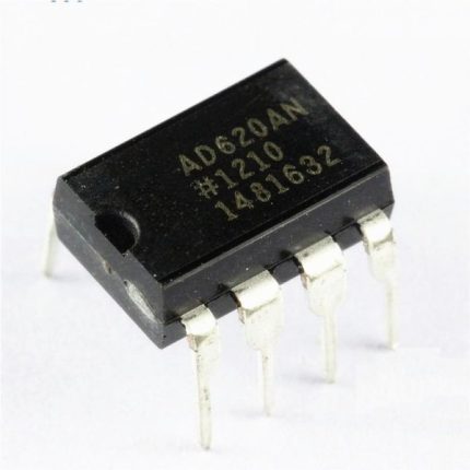
AD620AN IC Price in Pakistan
AD620 is an instrumentation amplifier which is low cost and high accuracy. It requires an external resister to set gain of 1 to 10,000. AD620 is 8 lead SOIC and DIP packaging and it is smaller than other designs and offers lower power. It supports 1.3mA max supply current. And it is good for battery power, for portable applications. AD620 Instrumentation Amplifier now in Pakistan
Reviews
There are no reviews yet.