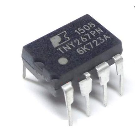
The TNY268 integrates a 700 V power MOSFET, oscillator, high voltage switched current source, current limit, and thermal shutdown circuitry onto a monolithic device IC. The start-up and operating power are derived directly from the voltage on the DRAIN pin, eliminating the need for a bias winding and associated circuitry. In addition, the TNY268 device incorporates auto-restart, line under-voltage sense, and frequency jittering. An innovative design minimizes audio frequency components in the simple ON/OFF control scheme to practically eliminate audible noise with standard taped/varnished transformer construction.
The fully integrated auto-restart circuit safely limits output power during fault conditions such as output short circuit or open loop, reducing component count and secondary feedback circuitry cost. An optional line sense resistor externally programs a line undervoltage threshold, which eliminates power down glitches caused by the slow discharge of input storage capacitors present in applications such as standby supplies. The operating frequency of 132 kHz is jittered to significantly reduce both the quasi-peak and average EMI, minimizing filtering cost.
-3%

TNY267 Power Integrations AC/DC Converters
Original price was: ₨ 250.₨ 200Current price is: ₨ 200.
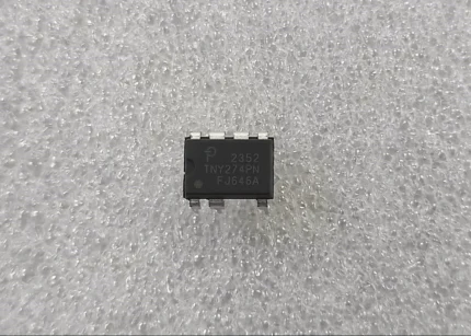
TNY274PN Power Integrations Off-Line Switcher IC
Original price was: ₨ 250.₨ 200Current price is: ₨ 200.
Tny268 Power Integrations Off-Line Switcher Ic
Original price was: ₨ 200.₨ 195Current price is: ₨ 195.
Description
Reviews (0)
Shipping & Delivery


Related products
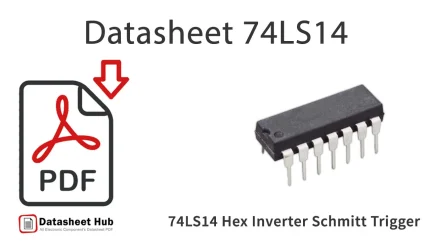
7414 74ls14 Schmitt Trigger Hex Inverter Ic In Pakistan
The 74LS14 Schmitt Trigger Hex Inverter IC is widely used in the following applications:
Noise Removal: Cleans up noisy signals in circuits, ensuring reliable digital operation.
Signal Conditioning: Used to sharpen slow input signals, making them suitable for digital logic systems.
Power Meters and Power Analyzers: In power measurement devices, the Schmitt trigger helps in ensuring stable, noise-free signal processing.
Signal Converters: Converts slow or noisy analog signals into clean digital signals.
Digital Systems: Used in systems requiring high noise immunity and stable, clean logic transitions.
Package Includes:
1 x 74LS14 Schmitt Trigger Hex Inverter IC (DIP-14)
Buy 74LS14 Schmitt Trigger Hex Inverter IC in Pakistan
G
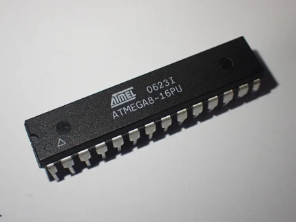
Atmega8l Atmega8 28pin Microcontroller
The ATMega8 Microcontroller AVR core combines a rich instruction set with 32 general-purpose working registers. All 32 registers are directly connected to the Arithmetic Logic Unit (ALU), allowing two independent registers to be accessed in one single instruction executed in one clock cycle. The resulting architecture is more code efficient while achieving throughputs up to ten times faster than conventional CISC microcontrollers.
The ATmega8 provides the following features: 8 Kbytes of In-System Programmable Flash with Read-While-Write capabilities, 512 bytes of EEPROM, 1 Kbyte of SRAM, 23 general purpose I/O lines, 32 general purpose working registers, three flexible Timer/Counters with compare modes, internal and external interrupts, a serial programmable USART, a byte-oriented Twowire Serial Interface, a 6-channel ADC (eight channels in TQFP and QFN/MLF packages) with 10-bit accuracy, a programmable Watchdog Timer with Internal Oscillator, an SPI serial port, and five software selectable power saving modes. The Idle mode stops the CPU while allowing the SRAM, Timer/Counters, SPI port, and interrupt system to continue functioning.
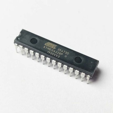
Original Atmega328 28 Pin Atmega328p-pu Microcontroller
Specifications of Atmel 8 Bit 28 Pins Microcontroller ATMEGA328P Microchip:
4.5V-5.5V operating range
Up to 20MHz
Part: ATMEGA328P-AU
32kB Flash program memory
1kB EEPROM
2kB Internal SRAM
Two8-bit Timer/Counters
One16-bit Timer/Counter
RTC with separate oscillator
6 PWM Channels
8 Channel 10-bit ADC
Serial USART
Master/Slave SPI interface
2-wire (I2C) interface
Watchdog timer
Analog comparator
23 IO lines
Data retention: 20 years at 85oC/ 100 years at 25oC
Reviews
There are no reviews yet.