The IR2112 is a high voltage IC that acts as a MOSFET driver and IGBT driver. It has independent high and low side referenced output channels with a threshold voltage of 600 V. Bootstrap feature makes it compatible for high side driver applications. Additionally, it has Schmitt triggered inputs that are compatible to the standard CMOS and LSTTL outputs. IR2112 is basically a low and high side driver IC with a voltage range of 10V to 20V..
-13%

IR2111-DIP8 Circuito Integrado Controlador Fuente Conmutada Tipo Llc
Original price was: ₨ 400.₨ 350Current price is: ₨ 350.
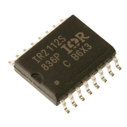
IR2112 SMD IR2112S IR 2112 IC Side Mosfet IGBT Driver Sop-16 2112S
Original price was: ₨ 450.₨ 400Current price is: ₨ 400.
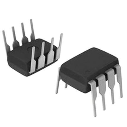
IR 2112 DIP STRPBF IOR HIGH AND LOW SIDE DRIVER
Original price was: ₨ 400.₨ 350Current price is: ₨ 350.
Description
Reviews (0)
Shipping & Delivery


Related products
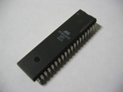
Atmega32 Atmega32a Atmega 32
Operating Voltage: 4.5V to 5V
Advanced RISC Architecture.
32 x 8 General Purpose Working Registers.
Fully Static Operation.
Up to 16 MIPS Throughput at 16 MHz.
On-chip 2-cycle Multiplier.
High Endurance Non-volatile Memory segments.
32 Kbytes of In-System Self-programmable Flash program memory.
1024 Bytes EEPROM.
2 Kbyte Internal SRAM.
Write/Erase Cycles: 10,000 Flash/100,000 EEPROM.
Data retention: 20 years at 85°C/100 years at 25°C(1).
Optional Boot Code Section with Independent Lock Bits.
In-System Programming by On-chip Boot Program.
True Read-While-Write Operation.
Programming Lock for Software Security.
Extensive On-chip Debug Support.
8 Single-ended Channels.
Byte-oriented Two-wire Serial Interface.
Programmable Serial USART.
Master/Slave SPI Serial Interface.
Programmable Watchdog Timer with Separate On-chip Oscillator.
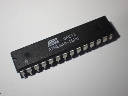
Atmega8l Atmega8 28pin Microcontroller
The ATMega8 Microcontroller AVR core combines a rich instruction set with 32 general-purpose working registers. All 32 registers are directly connected to the Arithmetic Logic Unit (ALU), allowing two independent registers to be accessed in one single instruction executed in one clock cycle. The resulting architecture is more code efficient while achieving throughputs up to ten times faster than conventional CISC microcontrollers.
The ATmega8 provides the following features: 8 Kbytes of In-System Programmable Flash with Read-While-Write capabilities, 512 bytes of EEPROM, 1 Kbyte of SRAM, 23 general purpose I/O lines, 32 general purpose working registers, three flexible Timer/Counters with compare modes, internal and external interrupts, a serial programmable USART, a byte-oriented Twowire Serial Interface, a 6-channel ADC (eight channels in TQFP and QFN/MLF packages) with 10-bit accuracy, a programmable Watchdog Timer with Internal Oscillator, an SPI serial port, and five software selectable power saving modes. The Idle mode stops the CPU while allowing the SRAM, Timer/Counters, SPI port, and interrupt system to continue functioning.
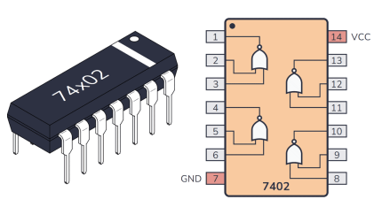
NOR Gate IC 74LS02 Quad 2-input
Operating voltage range: +4.75 to +5.25V
Maximum supply voltage: 7V
Maximum current allowed to draw through each gate output: 8mA
TTL outputs
Low power consumption
Maximum ESD: 3.5KV
Typical Rise Time: 15ns
Typical Fall Time: 15ns
Operating temperature :0°C to 70°C
Storage Temperature: -65°C to 150°C
Operating temperature: 0°C to 75°C
Pin Number Description
NORGATE 1
2 1A-INPUT1 of GATE 1
3 1B-INPUT2 of GATE 1
1 1Y-OUTPUT of GATE1
NORGATE 2
5 2A-INPUT1 of GATE 2
6 2B-INPUT2 of GATE 2
4 2Y-OUTPUT of GATE2
NORGATE 3
8 3A-INPUT1 of GATE 3
9 3B-INPUT2 of GATE 3
10 3Y-OUTPUT of GATE3
NORGATE 4
11 4A-INPUT1 of GATE 4
12 4B-INPUT2 of GATE 4
13 4Y-OUTPUT of GATE4
SHARED TERMINALS
7 GND- Connected to ground
14 VCC-Connected to positive voltage to provide power to all four gates
SKU: 0401 Categories: Discrete Electronic Components, ICs, Logic Gates Tags: 2input, 74LS02, Gate, IC, NOR, quad
Reviews
There are no reviews yet.