The CD4050 is a logic level conversion IC with six non-inverting hex buffers. This device supports logic level conversion while only requiring a single supply voltage (Vcc). When this IC is used for logic level conversion, the input signal high level (VIH) can exceed the Vcc supply voltage. The CD4050 IC is intended for use as a hex buffer, CMOS to TTL conversion and vice versa, CMOS current driver and CMOS High-to-Low Logic Level Converters. It can operate in 5V, 10V and 15V with a maximum input current of 1uA when operating at 18V. CD4049 is it’s complimentary inverting hex buffer IC.
-29%

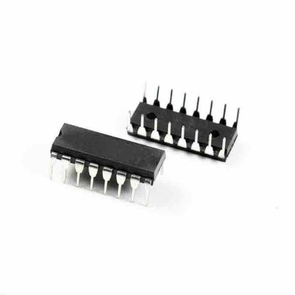
CD4049 Hex Inverter Buffer IC
Original price was: ₨ 120.₨ 90Current price is: ₨ 90.
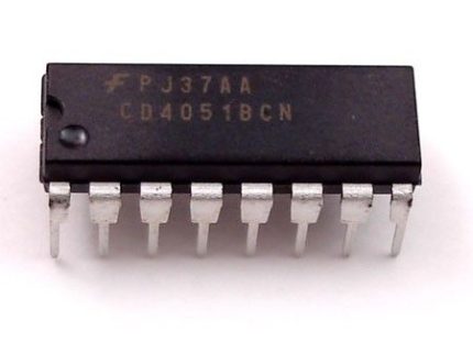
Cd4051b Cmos Single 8-channel Analog Multiplexer/demultiplexer
Original price was: ₨ 120.₨ 90Current price is: ₨ 90.
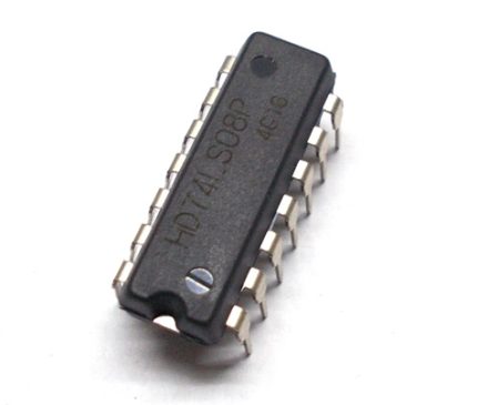
CD4050 – Hex Buffer Converter IC
Original price was: ₨ 120.₨ 85Current price is: ₨ 85.
Description
Reviews (0)
Shipping & Delivery


Related products
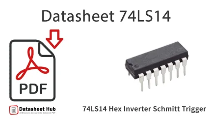
7414 74ls14 Schmitt Trigger Hex Inverter Ic In Pakistan
The 74LS14 Schmitt Trigger Hex Inverter IC is widely used in the following applications:
Noise Removal: Cleans up noisy signals in circuits, ensuring reliable digital operation.
Signal Conditioning: Used to sharpen slow input signals, making them suitable for digital logic systems.
Power Meters and Power Analyzers: In power measurement devices, the Schmitt trigger helps in ensuring stable, noise-free signal processing.
Signal Converters: Converts slow or noisy analog signals into clean digital signals.
Digital Systems: Used in systems requiring high noise immunity and stable, clean logic transitions.
Package Includes:
1 x 74LS14 Schmitt Trigger Hex Inverter IC (DIP-14)
Buy 74LS14 Schmitt Trigger Hex Inverter IC in Pakistan
G
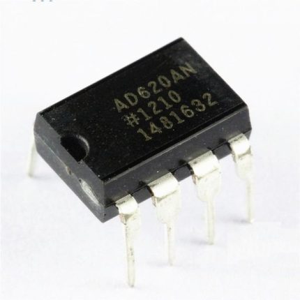
AD620AN IC Price in Pakistan
AD620 is an instrumentation amplifier which is low cost and high accuracy. It requires an external resister to set gain of 1 to 10,000. AD620 is 8 lead SOIC and DIP packaging and it is smaller than other designs and offers lower power. It supports 1.3mA max supply current. And it is good for battery power, for portable applications. AD620 Instrumentation Amplifier now in Pakistan
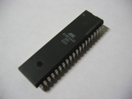
Atmega32 Atmega32a Atmega 32
Operating Voltage: 4.5V to 5V
Advanced RISC Architecture.
32 x 8 General Purpose Working Registers.
Fully Static Operation.
Up to 16 MIPS Throughput at 16 MHz.
On-chip 2-cycle Multiplier.
High Endurance Non-volatile Memory segments.
32 Kbytes of In-System Self-programmable Flash program memory.
1024 Bytes EEPROM.
2 Kbyte Internal SRAM.
Write/Erase Cycles: 10,000 Flash/100,000 EEPROM.
Data retention: 20 years at 85°C/100 years at 25°C(1).
Optional Boot Code Section with Independent Lock Bits.
In-System Programming by On-chip Boot Program.
True Read-While-Write Operation.
Programming Lock for Software Security.
Extensive On-chip Debug Support.
8 Single-ended Channels.
Byte-oriented Two-wire Serial Interface.
Programmable Serial USART.
Master/Slave SPI Serial Interface.
Programmable Watchdog Timer with Separate On-chip Oscillator.
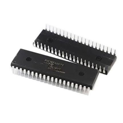
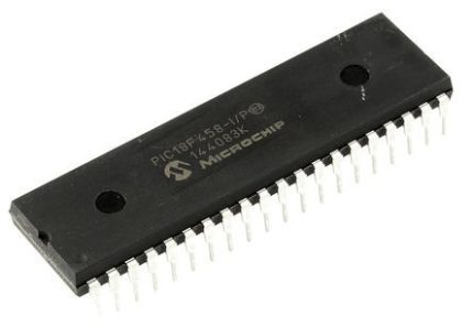
PIC 18F46K22
Sleep mode: 100 nA, typical
Watchdog Timer: 500 nA, typical
Timer1 Oscillator: 500 nA @ typical 32 kHz Flexible Oscillator Structure
Precision 16 MHz internal oscillator block:
Factory calibrated to 1%
Software selectable frequencies range of 31 kHz to 16 MHz
64 MHz performance available using PLL
No external components required
Four Crystal modes up to 64 MHz
Two external Clock modes up to 64 MHz
4X Phase Lock Loop (PLL)
Secondary oscillator using Timer1 @ 32 kHz
Fail-Safe Clock Monitor: Allows for safe shutdown if peripheral clock stops
Two-Speed Oscillator Start-up
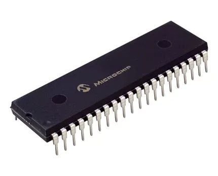
PIC16f877A 16f877A 16f 877A Microchip 40 Pin Microcontroller
FAQs
What is a PIC16f877A microcontroller?
What kind of applications is the PIC16f877A suitable for?
Does this chip need any additional components to function?
How do I program the PIC16f877A?
What is the pin configuration of this IC?
PIC microcontroller development board
Buy PIC16F877A online Pakistan
PIC16F877A microcontroller tutorial
Best PIC16F877A projects
PIC16F877A datasheet
PIC16F877A programming
PIC16F877A microcontroller for beginners
Arduino vs
Reviews
There are no reviews yet.