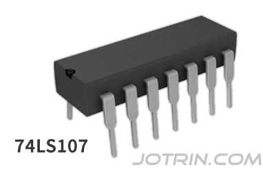
The 74LS107 has two inputs, J and K, which determine the state of the flip-flop. 74LS107 can set it (Q = 1), reset (Q = 0), or left unchanged. that also has a clock (CLK) and preset (PR) inputs, which control when the inputs are evaluated and when the outputs change.
The 74LS107 is a 74LS-series device, which means it is a low-power, high-speed logic device based on transistor-transistor logic (TTL) technology. It is widely used in digital electronics applications because of its low power consumption, fast switching speeds, and ease of use.
Features of 74LS107
Dual Design
Easy to use
High-speed Device
Clock and Preset inputs
Low Power Consumption
Dual JK Flip Flop Package IC
More Flexible Control of J-K input
Application of 74LS107
Counters
Shift Registers
State Machines
Digital Filters
Timing Circuits
Storage Elements
74LS107 Pinout
image.png
Pin Description of 74LS76:
The 74LS107 Dual J-K Flip-Flop has a total of 14 pins, which include inputs for two independent J-K flip-flops (1 J, 1 K, 2 J, and 2 K ), clock inputs for both flip-flops (1 CLKA and 2 CLK), outputs for both flip-flops (1 Q, 2 Q), and complementary outputs for both flip-flops (1 Q and 2 Q). The device also has power and ground connections (V CC and GND).
The inputs and outputs allow for the state of the flip-flops to be updated and monitored. The power and ground connections provide power to the device for operation.
74LS107 Equivalent: 74HC107, 74F107, 74ACT107
When selecting an equivalent device, it’s important to carefully consider the application’s specific requirements to ensure that the equivalent device meets the necessary specifications. In general, the choice of an equivalent device will depend on factors such as the desired operating speed, power consumption, and noise immunity.
74LS107 Alternative: 74LS73, 74LS109, 74LS113
How to use 74LS107?
The 74LS107 Dual J-K Flip-Flop is a simple digital device that can store a binary state (1 or 0) based on the state of its inputs. To use the 74LS107, you will need to connect the inputs and outputs to your desired circuit. Here’s a general outline of how to use the 74LS107:
Power Supply: Connect the power supply to the V CC and GND pins. The device operates with a power supply voltage of 5V.
Inputs: Connect each flip-flop’s J and K inputs to the desired signal sources. The inputs should be connected to a logic high (1) or logic low (0) signal.
Clock Inputs: Connect the clock inputs (CLKA and CLKB) to the desired clock signal sources. The clock signal should be connected to a square wave that toggles between logic high and logic low.
Outputs: Connect each flip-flop’s Q and Q outputs to the desired destination. The outputs will reflect the binary state stored in the flip-flops.
Timing: The timing of the 74LS107 is controlled by the clock inputs. The device updates the state of the flip-flops on the rising edge of the clock signal.
Truth Table: To understand how the 74LS107 operates, it’s useful to consult the truth table for the device. The truth table will show how the outputs respond to different combinations of inputs.
The 74LS107 is a straightforward device. To use the device effectively, it’s important to understand its input and output specifications and carefully design the associated timing and control signals.
Where to use 74LS107 Dual J-K Flip-Flop?
The 74LS76 Dual J-K Flip-Flop is commonly used in digital circuits for data storage, sequential logic, and clock division. As a data storage device, the 74LS76 can be used to store binary signals and control other parts of the circuit. In sequential logic applications, the 74LS76 is used to store the circuit’s state and control the sequence’s progression. Additionally, the 74LS76 can divide a clock signal into slower or faster signals, making it useful for various clock division applications.
The 74LS76 is versatile, fast, and efficient, making it a popular choice for many digital circuit applications.
Why is the 74LS107 Important for Digital Electronics Design?
The 74LS107 is important in digital electronics design due to its versatility, speed, and reliability. As a dual J-K flip-flop, it can be used in various digital circuits, making it a useful component for many digital design projects. Its fast propagation delay of around 15 ns makes it well-suited for high-speed digital circuits. In contrast, its high noise immunity and low power consumption make it a reliable choice for many applications.




Reviews
There are no reviews yet.