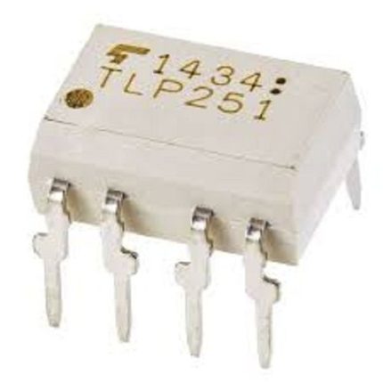
TLP250’s pin layout is as follows. It is clearly shows in the figure that led at the input stage and photodetector diode at the output stage is use to provide isolation between input and output.
Firstly Pin number 1 and 4 are not connect to any point. Hence they are not in use. Pin 2 is an anode point of input stage light-emitting diode however pin 3 is the cathode point of the input stage. Input is provided to pin 2 and 3. Pin 8 is for supply connection. Pin 5 is for the ground of power supply.As shown in figure above input is drive signal that drives the output. Vin is according to signal ground. It should not be connect with supply ground and output ground. It is clearly shows in above figure TLP250 and load ground is refererence to the power ground and it is isolated from input signal reference ground.
When input is high, MOSFET Q1 get high signal from TLP250 and it is drive by power supply and current flows through the load. When input is low, MOSFET Q1 get low signal from TLP250 output pin and mosfet Q1 remains off and there is no current flow to load.
Value of supply voltage ranges between 10-15 volts. Usually input signal is provided through microcontroller and microcontroller input signal level is in the order of 5 volt. C1 decouples the circuit as the capacitor.
TLP250 as a high side MOSFET driver
Circuit diagram of MOSFT driver tlp250 used as high side driver is as follows. It is using as non inverting high side mosfet driver. Because input signal ground is connect to cathode of input stage light emitting diode. Therefore it is use as a non inverting high side mosfet driver.







Reviews
There are no reviews yet.