Low-voltage and Standard-voltage Operation
2.7 (VCC = 2.7V to 5.5V)
1.8 (VCC = 1.8V to 5.5V)
Internally Organized 128 x 8 (1K), 256 x 8 (2K), 512 x 8 (4K),
1024 x 8 (8K) or 2048 x 8 (16K)
Two-wire Serial Interface
Schmitt Trigger, Filtered Inputs for Noise Suppression
Bidirectional Data Transfer Protocol
100 kHz (1.8V) and 400 kHz (2.7V, 5V) Compatibility
Write Protect Pin for Hardware Data Protection
8-byte Page (1K, 2K), 16-byte Page (4K, 8K, 16K) Write Modes
Partial Page Writes Allowed
Self-timed Write Cycle (5 ms max)
High-reliability
Endurance: 1 Million Write Cycles
Data Retention: 100 Years
Automotive Devices Available
8-lead JEDEC PDIP, 8-lead JEDEC SOIC, 8-lead Ultra Thin Mini-MAP (MLP 2×3), 5-lead SOT23, 8-lead TSSOP and 8-ball dBGA2 Packages
Die Sales: Wafer Form, Waffle Pack and Bumped Wafers
-28%

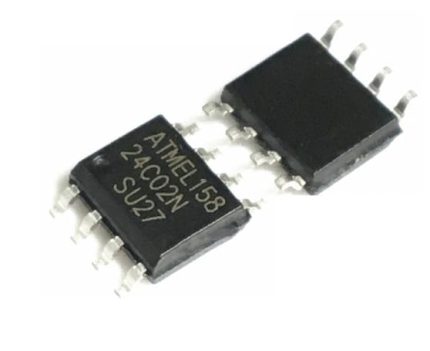
At24c02bn SMD 24c02 SMD Eeprom Memory IC
Original price was: ₨ 120.₨ 75Current price is: ₨ 75.
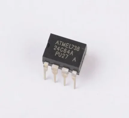
24c64 Serial Eeprom 64k Memory Ic
Original price was: ₨ 90.₨ 65Current price is: ₨ 65.
Serial EEPROM AT24C02
Original price was: ₨ 90.₨ 65Current price is: ₨ 65.
Description
Reviews (0)
Shipping & Delivery


Related products
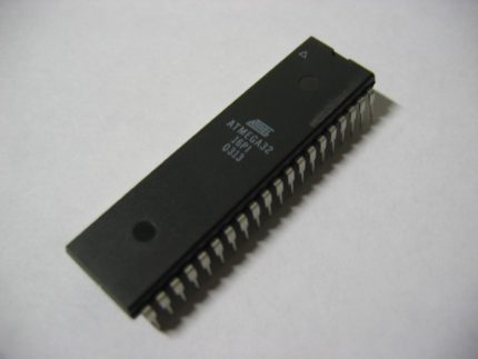
Atmega32 Atmega32a Atmega 32
Operating Voltage: 4.5V to 5V
Advanced RISC Architecture.
32 x 8 General Purpose Working Registers.
Fully Static Operation.
Up to 16 MIPS Throughput at 16 MHz.
On-chip 2-cycle Multiplier.
High Endurance Non-volatile Memory segments.
32 Kbytes of In-System Self-programmable Flash program memory.
1024 Bytes EEPROM.
2 Kbyte Internal SRAM.
Write/Erase Cycles: 10,000 Flash/100,000 EEPROM.
Data retention: 20 years at 85°C/100 years at 25°C(1).
Optional Boot Code Section with Independent Lock Bits.
In-System Programming by On-chip Boot Program.
True Read-While-Write Operation.
Programming Lock for Software Security.
Extensive On-chip Debug Support.
8 Single-ended Channels.
Byte-oriented Two-wire Serial Interface.
Programmable Serial USART.
Master/Slave SPI Serial Interface.
Programmable Watchdog Timer with Separate On-chip Oscillator.
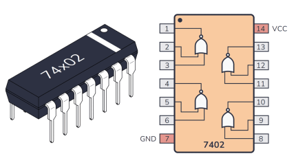
NOR Gate IC 74LS02 Quad 2-input
Operating voltage range: +4.75 to +5.25V
Maximum supply voltage: 7V
Maximum current allowed to draw through each gate output: 8mA
TTL outputs
Low power consumption
Maximum ESD: 3.5KV
Typical Rise Time: 15ns
Typical Fall Time: 15ns
Operating temperature :0°C to 70°C
Storage Temperature: -65°C to 150°C
Operating temperature: 0°C to 75°C
Pin Number Description
NORGATE 1
2 1A-INPUT1 of GATE 1
3 1B-INPUT2 of GATE 1
1 1Y-OUTPUT of GATE1
NORGATE 2
5 2A-INPUT1 of GATE 2
6 2B-INPUT2 of GATE 2
4 2Y-OUTPUT of GATE2
NORGATE 3
8 3A-INPUT1 of GATE 3
9 3B-INPUT2 of GATE 3
10 3Y-OUTPUT of GATE3
NORGATE 4
11 4A-INPUT1 of GATE 4
12 4B-INPUT2 of GATE 4
13 4Y-OUTPUT of GATE4
SHARED TERMINALS
7 GND- Connected to ground
14 VCC-Connected to positive voltage to provide power to all four gates
SKU: 0401 Categories: Discrete Electronic Components, ICs, Logic Gates Tags: 2input, 74LS02, Gate, IC, NOR, quad
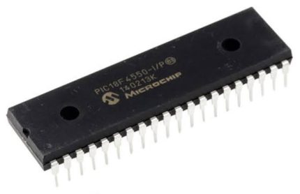
PIC 18F46K22
Sleep mode: 100 nA, typical
Watchdog Timer: 500 nA, typical
Timer1 Oscillator: 500 nA @ typical 32 kHz Flexible Oscillator Structure
Precision 16 MHz internal oscillator block:
Factory calibrated to 1%
Software selectable frequencies range of 31 kHz to 16 MHz
64 MHz performance available using PLL
No external components required
Four Crystal modes up to 64 MHz
Two external Clock modes up to 64 MHz
4X Phase Lock Loop (PLL)
Secondary oscillator using Timer1 @ 32 kHz
Fail-Safe Clock Monitor: Allows for safe shutdown if peripheral clock stops
Two-Speed Oscillator Start-up
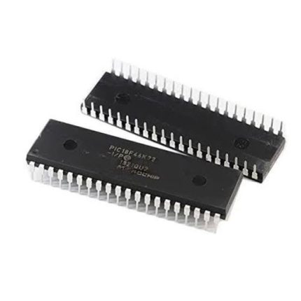
PIC16f877A 16f877A 16f 877A Microchip 40 Pin Microcontroller
FAQs
What is a PIC16f877A microcontroller?
What kind of applications is the PIC16f877A suitable for?
Does this chip need any additional components to function?
How do I program the PIC16f877A?
What is the pin configuration of this IC?
PIC microcontroller development board
Buy PIC16F877A online Pakistan
PIC16F877A microcontroller tutorial
Best PIC16F877A projects
PIC16F877A datasheet
PIC16F877A programming
PIC16F877A microcontroller for beginners
Arduino vs
Reviews
There are no reviews yet.